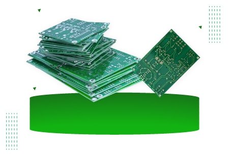
Holes are drilled on the board and then the electronic components are fixed. Thereafter, the electronic components are soldered in correct positions so that copper tracks along with the components form a circuit. These printed circuit boards are used in electronic products including wireless devices, automotive, and robotic appliances and they provide quick access, functioning, monitoring, control, and precise results when compared to wiring based devices. We have been helping students by providing them with top-quality online help with assignment on Circuit Board Layout that can assist you secure top grades.
Most of our writers are holders of Ph.D. degree and they have spent many years in this field providing them an edge.
The Designing Process of a Printed Circuit Board
Depending on the printed circuit board, there are several ways to design a PCB. A circuit board design is created as a bulk using multiple machines in a PCB fabrication industry such as punching, drilling, plating, and fabrication method performed by automated machines. Laser drilling with automatic plating machines, CNC machines, strip etching machines and using flying probe testers, optical inspection equipment for testing of PCB produce top-quality PCBs.
The steps are discussed in our Circuit Board Layout assignment help online as follows:
Designing the PCB with a software: Draw a circuit diagram using the PCB layout software including CAD software, Multisim software, and Eagle. This kind of PCB software has many components, which are used for building a circuit. You can change the design of the circuit and modify it as per your requirement and convenience.
Film generation: A film is generated from the diagram of a circuit board of a PCB layout software that is sent to a manufacturing unit where negative images are printed on a plastic sheet.
Raw Materials selection: A major portion of printed circuit boards is made of unbreakable fiberglass or glass that has copper foil and bonded into either one side or both sides of the board. The PCBs that are made from paper phenolic along with a copper foil are less expensive and used in electrical devices.
Drill holes: Machines are used for putting holes on the PCBs. Two kinds of machines are used for drilling the PCBs; CNC machines and hand machines. CNCs are computer-based machines that run manually and automatically whereas hand machines need human intervention to drill holes. After the PCB boards are put into the CNC machines, holes are drilled as per the decided pattern and PCBs are placed.
Apply image: The PCBs are printed in various ways such as manual pen, pen plotters, dry transfers, and printers. For printing the layouts on PCD, laser printers are a better option.
Stripping and Etching: The process includes the removal of unwired copper using various kinds of chemicals including ammonium per-sulphate, ferric chloride, etc. The PCB is placed in a chemical bowl and then cleaned using a brush.
Testing: After the manufacturing process of the PCB is completed, testing is done for checking whether it is working properly. These days, several automatic testing equipments are there to perform high-volume PCB testing.
These are discussed properly when you buy assignment help on Circuit Board Layout topic.


 3 Bellbridge Dr, Hoppers Crossing, Melbourne VIC 3029